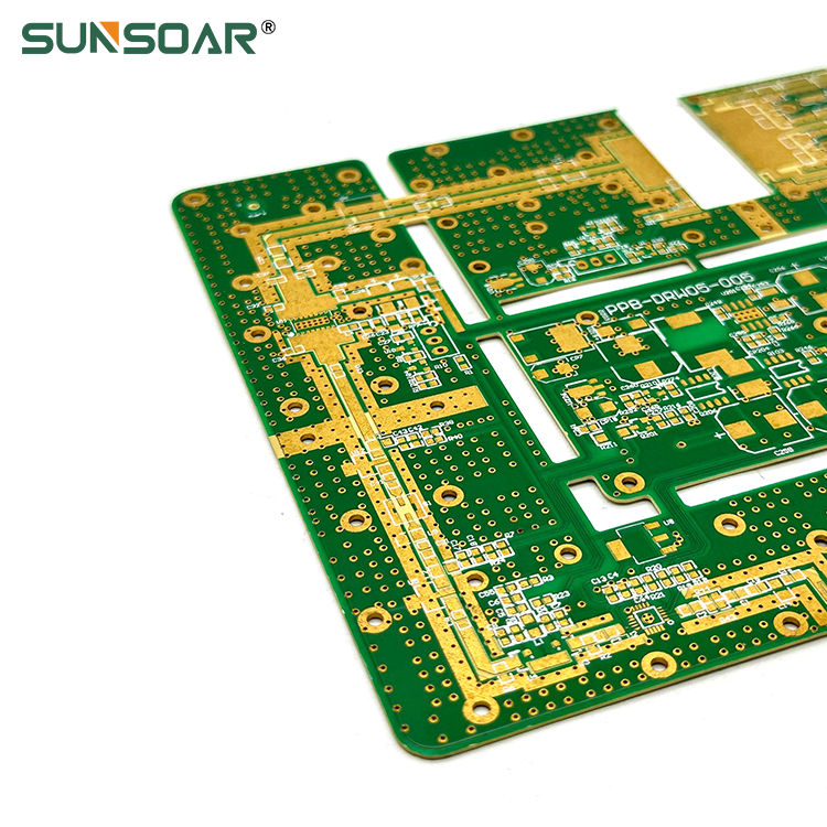
Optimizing PCB/PCBA Design for High-Speed Applications: Key Considerations for Engineers
- Sunsoar Engineer Hannah
- Sep 3, 2024
- 3 min read
In today's fast-paced electronics industry, designing for high-speed applications is crucial. Whether it's for telecommunications, automotive systems, or consumer electronics, engineers must focus on optimizing PCB (Printed Circuit Board) and PCBA (Printed Circuit Board Assembly) designs to ensure performance and reliability. With higher clock speeds and tighter component layouts, signal integrity becomes a critical factor. Below are some key considerations engineers should keep in mind when tackling high-speed PCB designs.
1. Controlled Impedance
Maintaining controlled impedance is essential for high-speed circuits to ensure signal integrity. Variations in impedance can cause signal reflections, leading to data loss or corruption, especially at higher frequencies. Engineers need to carefully design the PCB trace width, spacing, and choose appropriate materials to manage impedance effectively.
Best Practice: Utilize advanced simulation tools to calculate the exact trace dimensions and dielectric constants needed to maintain consistent impedance across the PCB.
2. Minimizing Crosstalk
Crosstalk occurs when adjacent signal traces interfere with each other, a significant issue in high-speed designs. Crosstalk can degrade signals, causing errors in data transmission.
Best Practice: Increase the spacing between high-speed traces, or use differential pair routing where two complementary signals are routed closely together to reduce the risk of crosstalk.
3. Reducing Electromagnetic Interference (EMI)
High-speed circuits are more prone to electromagnetic interference (EMI), which can lead to signal distortion and affect the overall performance of the PCB. EMI can originate from external sources or even from within the PCB itself.
Best Practice: Shielding and proper grounding techniques can greatly reduce EMI. Using a ground plane effectively, keeping traces short, and placing sensitive components away from noise sources are critical steps to minimize interference.
4. Layer Stack-Up and Routing
The layer stack-up of a PCB plays a critical role in its overall performance, especially in high-speed designs. Most high-speed PCBs require multiple layers to facilitate proper signal routing and ensure that signal integrity is maintained.
Best Practice: Use a balanced layer stack-up with alternating signal and ground layers. This helps control impedance and minimizes noise. High-speed signal traces should ideally be routed on internal layers where they are less susceptible to external interference.
5. Power Integrity
In high-speed designs, power integrity is just as important as signal integrity. Poor power distribution can result in voltage drops, noise, and power fluctuations, which affect the performance of high-speed components.
Best Practice: Place decoupling capacitors close to the power pins of components to smooth out power fluctuations. A solid ground plane can also reduce impedance in the power distribution network, ensuring stable power delivery.
6. Thermal Management
High-speed PCBs generate more heat due to increased power consumption, which can affect component performance and lifespan. Managing heat is crucial to ensuring long-term reliability.
Best Practice: Use thermal vias, heat sinks, and ensure proper airflow to manage heat effectively. This helps to maintain a safe operating temperature for the PCB.
Leveraging Advanced Tools
With the complexity of high-speed PCB design, advanced simulation tools are indispensable. They allow engineers to model signal behavior, predict potential issues like EMI or crosstalk, and optimize the design before moving into production.
Conclusion
Designing PCBs for high-speed applications requires a deep understanding of how signals behave at high frequencies. Engineers need to focus on controlled impedance, crosstalk minimization, EMI reduction, proper layer stack-up, and power integrity to ensure optimal performance. As technology continues to evolve, staying informed about the latest tools and best practices will be key to developing reliable and efficient high-speed PCBs.


Comments