Exploring the Impact of Line Width and Spacing on PCB Signal Integrity
- Sunsoar engineer Mia
- Mar 27
- 2 min read
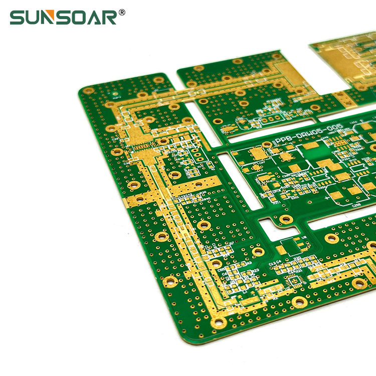
In PCB (Printed Circuit Board) design, the line width and spacing play a crucial role in ensuring signal integrity, preventing crosstalk, and reducing electromagnetic interference (EMI). As electronic devices become more complex and operate at higher frequencies, proper management of trace width and spacing is essential to maintaining performance and reliability.
Why Line Width and Spacing Matter
1. Signal Integrity and Resistance Control
The width of a PCB trace determines its electrical resistance. Narrow traces have higher resistance, which can lead to voltage drops and signal degradation, especially in high-speed circuits. Conversely, wider traces reduce resistance, allowing signals to travel with minimal loss.
2. Managing Crosstalk and Electromagnetic Interference (EMI)
Crosstalk occurs when signals from adjacent traces interfere with each other, leading to data corruption and unpredictable circuit behavior. Increasing the spacing between traces helps reduce this unwanted interaction by minimizing capacitive and inductive coupling.
3. Controlling Impedance for High-Speed Signals
For high-speed PCB designs, maintaining consistent impedance is critical to avoiding signal reflections and ensuring data integrity. The width of a trace, its height above the ground plane, and the dielectric material all contribute to impedance. Precise control over line width and spacing ensures that signals propagate as intended without excessive loss or distortion.
Optimizing Line Width and Spacing for Different PCB Types
1. Standard PCBs (Low-Frequency Designs)
Trace width: Typically 0.15–0.20 mm for signal traces
Spacing: 0.20 mm or more between adjacent traces
Copper thickness: 1 oz (35 µm) is common for general applications
2. High-Frequency and High-Speed PCBs
Trace width: Depends on the target impedance, often controlled using PCB stack-up and controlled impedance calculations
Spacing: 3–5 times the trace width to minimize crosstalk
Use of ground planes and shielding techniques to improve signal integrity
3. Power and High-Current PCBs
Trace width: Wider traces (e.g., 1.0 mm or more) for carrying high current without excessive heating
Spacing: Larger clearance to prevent arcing and ensure reliability
Industry Standards and Design Guidelines
Several industry standards guide PCB designers in selecting appropriate trace widths and spacing:
IPC-2221: General standard for PCB design, providing minimum spacing rules
IPC-2152: Guidelines for determining trace widths based on current-carrying capacity
Controlled Impedance Design Rules: Used in high-speed PCB design to match impedance requirements
How Sunsoar PCB Ensures High-Quality PCB Design
At Sunsoar PCB, we implement advanced manufacturing and design techniques to optimize line width and spacing for superior signal integrity. Our expertise includes:
Controlled impedance PCBs for high-speed applications
HDI (High-Density Interconnect) boards with precise trace routing
Advanced simulation tools to predict and prevent signal integrity issues
For custom PCB design solutions, contact us at sales03@sunsoartech.com or call +86 13632793113.
Conclusion
The impact of line width and spacing on PCB signal integrity cannot be overstated. Properly designed traces help reduce resistance, prevent crosstalk, and ensure impedance consistency, leading to better-performing electronic devices. Whether designing a simple PCB or a high-speed, high-frequency board, understanding these factors is crucial to achieving reliable and efficient circuits.


Comments