Introduction
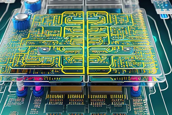
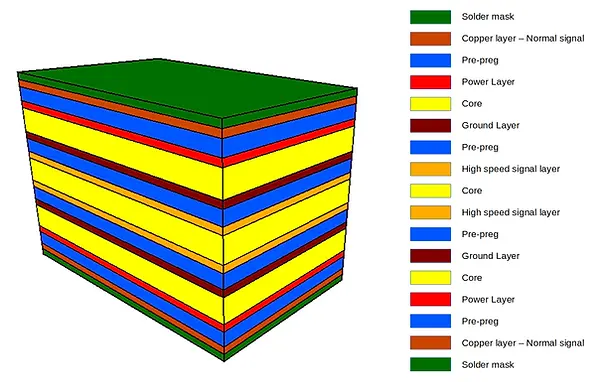
A multilayer printed circuit board (PCB) consists of two or more conductive copper layers separated by dielectric materials like FR-4. These PCBs enhance component density by allowing placement on both sides and internally buried layers, making them ideal for complex digital circuits, RF/microwave systems, high-speed computing, and other applications requiring high interconnectivity.
This article provides an in-depth overview of multilayer PCB technology, covering:
-
Multilayer PCB manufacturing processes
-
Materials and construction
-
Key design considerations
-
Modeling and analysis
-
Thermal management
-
Signal integrity
-
Cost tradeoffs
-
Reliability factors
Understanding multilayer PCB capabilities and design best practices is essential for leveraging their benefits in electronic product development.
-
What is Multilayer PCB: Manufacturing, Design and Cost ?
-
6 Layer PCB
-
8 Layer PCB
-
10 Layer PCB
-
12 Layer PCB
Multilayer PCB Manufacturing Process
Fabricating a multilayer PCB involves specialized sequential lamination processes to bond multiple double-sided circuit layers into a single consolidated board. The typical manufacturing steps include:
1. Inner Layer Formation
-
Photolithographic patterning to define circuit traces on treated copper-clad laminate.
-
Etching to remove unwanted copper, leaving behind the traces.
-
Adding layer registration targets and tooling holes.
-
Conducting electrical testing of traces.
-
Surface preparation for lamination.
2. Layer Lamination
-
Using sheet lamination presses to bond layers together.
-
Arranging stackup of cores, prepregs, copper, and dielectrics.
-
Curing under temperature and pressure to form the laminate.
3. Drill Holes
-
High precision drilling to create tooling and via holes.
-
Ensuring accurate registration to drill each layer precisely.
4. Hole Plating
-
Electroless copper plating as a thin conductive layer.
-
Electrolytic copper plating to achieve the desired thickness.
-
Copper builds up on inner layers and drilled holes.
5. Outer Layer Processing
-
Applying liquid photoimageable (LPI) solder mask.
-
Printing legends with identification markings.
-
Patterning and etching outer layer circuitry.
-
Panel routing into individual PCBs.
6. Testing and Quality Assurance
-
Automated optical inspection (AOI).
-
Net connectivity testing.
-
Impedance, high voltage, and functional testing.
-
Dimensional quality control.
These steps ensure the production of high-quality, reliable multilayer PCBs suitable for a wide range of advanced electronic applications.

Multilayer PCB Materials and Construction
Multilayer boards are composed of conductive copper layers separated by dielectric prepreg and core layers. Here are some typical material options:
Conductive Layers:
-
Rolled annealed copper foil (1/2 to 3 oz thickness)
-
Electrodeposited copper foil
-
Finishes: silver, gold, or nickel plating
Dielectric Layers:
-
FR-4 (glass-reinforced epoxy)
-
High Tg epoxy (for high temperature stability)
-
PTFE (Teflon) for RF/wireless boards
-
Polyimide (for flexible PCBs)
-
Cyanate ester (for radar and defense applications)
Bonding Layers:
-
FR-4 prepregs (partially cured resin)
-
Rogers prepregs
-
Fluoropolymer adhesive films
-
Reinforced and non-reinforced options
Common Multilayer Constructions:
-
4-6 layers: low to moderate complexity
-
8-10 layers: more complex digital boards
-
12-16 layers: advanced RF and data processing
-
20+ layers: extremely dense interconnections
-
60+ layers: state-of-the-art HDI technology
Multilayer PCB Design Considerations

Designing multilayer PCBs presents challenges due to higher interconnect density, thermal characteristics, fabrication constraints, and signal integrity factors. Here are key multilayer PCB design guidelines:
Board Stackup:
-
Select dielectric materials based on electrical, thermal, and CTE properties.
-
Model performance with various laminate combinations.
-
Use symmetric construction when possible.
-
Incorporate reference planes for each signal layer.
-
Assign plane layers judiciously (ground, power, signal).
High-Speed Routing:
-
Use impedance-controlled routing for high-speed nets.
-
Place sensitive traces between ground/power planes.
-
Match trace widths and spacing for differential pairs.
-
Minimize abrupt bends, stubs, and length mismatches.
-
Simulate performance in the applied environment.
Thermal Design:
-
Model hotspots and heat-spreading layers.
-
Incorporate thermal vias for heat conduction.
-
Use thicker copper planes for heat spreading.
-
Select dielectrics with good thermal conductivity.
-
Ensure proper component spacing and airflow.
Signal Integrity:
-
Optimize layer stackup to isolate noise coupling.
-
Assign return paths for high-speed traces.
-
Use plated-through holes for consistent returns.
-
Incorporate passive components like capacitors and resistors.
-
Include provisions for decoupling and terminations.
Power Distribution:
-
Provide adequate pinout for the number of supplies.
-
Use separate regulator areas for analog and digital circuits.
-
Provide bulk decoupling near supply sources.
-
Distribute power planes to minimize branch lengths.
Component Layout:
-
Place components on both sides for higher density.
-
Group components by type to simplify routing.
-
Ensure components fit within the board outline.
-
Provide access space for rework when needed.
-
Allow clearance for routing channels.
Layer Transitions:
-
Minimize layer changes when possible.
-
Use blind/buried vias for layer transitions.
-
Taper trace widths when changing layers.
-
Ensure smooth impedance transitions.
Testability:
-
Include test points, ports, and potential probes.
-
Provide a grid of test pads for bed-of-nails testing.
-
Add built-in test structures when possible.
-
Facilitate access to debug interface ports.
These guidelines ensure the reliability, performance, and manufacturability of multilayer PCBs, addressing the complexities of modern electronic designs.
Modeling and Analysis
Given the multiple interactions between material properties, stackup, component layout, and routing density, modeling tools are essential for effective multilayer PCB development:
Electromagnetic Simulation:
-
Model radiation, coupling, and resonances.
-
Detect issues with stackup, trace geometry, and splits.
-
Identify necessary shielding and ground planes.
Signal Integrity:
-
Analyze impedance discontinuities and reflections.
-
Verify termination strategies and transmission line effects.
-
Account for losses, noise, and coupling.
Power Integrity:
-
Model DC and AC supply characteristics.
-
Confirm power delivery network design.
-
Include effects of decoupling and PDN.
Thermal Analysis:
-
Predict temperature profiles under load.
-
Identify hotspots in component layout.
-
Model impacts of heat sinking and spreading.
Vibration/Shock Analysis:
-
Assess vibration modes and resonances.
-
Identify necessary mechanical reinforcement.
-
Verify component mounting and solder joint reliability.
DFX Analysis (Design for Excellence):
-
Check design for fabrication, assembly, and testing.
-
Assess serviceability and rework considerations.
-
Improve manufacturability, yield, and cost.
These modeling tools ensure the reliability, performance, and manufacturability of multilayer PCBs by addressing the complexities inherent in modern electronic designs.
Cost Considerations
Increasing multilayer PCB complexity leads to higher fabrication costs. Key factors include:
-
Layer Count: Each additional conductive layer increases costs due to more process steps for imaging, plating, and lamination.
-
Board Size: Larger boards require equipment with greater capacity, typically ranging from 24”x36” to 28”x44”.
-
Higher Density: Tighter trace and spacing tolerances, smaller hole sizes, and the use of thinner materials for more layers all contribute to increased costs. Complex panelization and breakouts also add to expenses.
-
Advanced Materials: Specialized materials such as low-loss laminates, thin core/prepregs, thicker copper, and stacked microvias are more expensive.
-
Low Volume: Non-recurring engineering charges apply to smaller production runs, which cannot leverage economies of scale.
Understanding these factors is crucial for effectively managing costs in multilayer PCB fabrication.
Cost Considerations
Key factors affecting multilayer PCB reliability include:
Fabrication Process Control:
-
Exceptional drill registration accuracy.
-
Stringent lamination quality to prevent voids.
-
Plating integrity for continuity and adhesion.
Laminate Quality:
-
High glass transition temperature (Tg).
-
Low coefficient of thermal expansion (CTE).
-
Minimal moisture absorption characteristics.
Design Factors:
-
Efficient internal layer heat dissipation.
-
Adequate mechanical reinforcement and stiffness.
-
Optimal component layout and density.
Testing and Inspection:
-
Automated optical inspection (AOI).
-
Comprehensive net connectivity, in-circuit, and functional testing.
-
X-ray analysis for internal structure evaluation.
-
Cross-sectioning to assess plating quality.
-
Environmental stress testing for temperature, humidity, and vibration resilience.
These factors are crucial for ensuring the reliability and performance of multilayer PCBs.
Cost Considerations
Multilayer PCB technology facilitates the creation of denser, higher-performance electronic designs by leveraging stacked circuit layers interconnected through plated holes and vias. Achieving these benefits demands proficiency in selecting and utilizing specialized materials, employing advanced modeling tools, and implementing sophisticated thermal and signal integrity techniques. Additionally, ensuring reliability through rigorous testing and mastering advanced manufacturing processes are critical. This article has provided a thorough overview of multilayer PCB capabilities, equipping engineers with the knowledge to effectively design, analyze, and produce robust multilayer boards that meet the stringent demands of modern electronics.
